
Empowering engineering education
We are dedicated to helping today’s engineering students prepare for tomorrow. Learn about the multi-disciplinary student engineering software, curriculum, training and tools we offer to empower the next generation of digital talent.


Supporting engineering education across the globe


Academic partner program
Do you want to teach your students some of the best, industry-strength engineering software, but don’t have access to it? Apply for a grant to get Siemens software to support your classroom. Academic institutions worldwide use this program to set their students up for success and to provide a strong pipeline of talent to enable digital enterprises.

Innovation in the Classroom
Listen to the discussions among leading voices in the engineering education sector. Learn their approaches as they prepare future engineers to shape the world of innovation.

Katholieke Universiteit Leuven
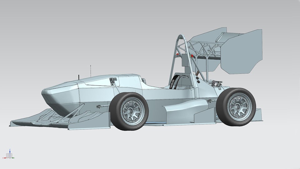
Belgian university uses Siemens solutions to educate future engineers in product design and manufacturing
Company:Katholieke Universiteit Leuven
Location:Leuven, Belgium
Siemens Software:NX, Simcenter 3D Solutions, Solid Edge, Teamcenter
How academia can close the skills gap
Stand out in today's competitive environment and learn how to close the engineering skills gap in the age of digitalization.
