
Valor
Valor Process Preparation
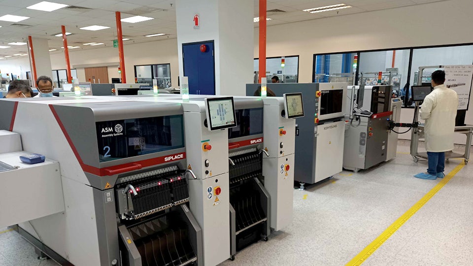
Creates a single, central database of all manufacturing process definitions and engineering data for all machine vendors and manufacturing sites, ensuring an error-free manufacturing process.

A single tool for all surface mount technology (SMT) process engineering tasks. SMT programming is made fast and easy with Valor software.
Simplify the delivery of high-quality, consistent SMT process collateral. Efficiently meet the process engineering demands of high-mix, low-volume production.
Valor Process Preparation creates a central database of all manufacturing process definitions and engineering data. This provides flexibility to move between machine vendors and manufacturing sites. Acting as a single environment for all manufacturing stages, this SMT programming tool ensures data is constantly up to date, and manufacturing is error-free.

Electronic manufacturing services (EMS) companies often provide quotes for projects that never make it into production. Valor BOM Connector reduces the time it takes to create accurate quotations for printed circuit board (PCB) assemblies. This minimizes the waste of valuable engineering hours.

Company:ESCATEC
Industry:Electronics, Semiconductor devices
Location:Penang, Malaysia
Siemens Software:Valor Parts Library, Valor Process Preparation
Get a single environment for manufacturing process engineering of all PCB assembly stages. Data is constantly up to date for an error-free manufacturing process.